Privacy statement: Your privacy is very important to Us. Our company promises not to disclose your personal information to any external company with out your explicit permission.
Application of High Performance Engineering Plastic PEEK/PPS in Semiconductor Field
Throughout the semiconductor manufacturing process, the role of plastics is mainly packaging and transmission, connecting various processing processes, preventing pollution and damage, optimizing pollution control, and improving the yield of key semiconductor manufacturing processes. The plastic materials used include PEEK, PPS, PP , ABS, PVC, PBT, PC , fluoroplastics, PAI, COP, etc. With the continuous development of semiconductor technology, the performance requirements of materials are also getting higher and higher.

1. CMP retaining ring
Chemical mechanical polishing (CMP) is a key process technology in the wafer production process. During the grinding process, the CMP retaining ring is used to fix the wafer and wafer. The selected material should have good wear resistance, dimensionally stable, chemical resistance, easy processing, and avoid scratches and contamination of the wafer/round surface.
CMP retaining rings are used to hold chips during grinding. The selected material should avoid scratches and contamination of the chip surface. It is usually made of standard Polyphenylene Sulfide.
PEEK has high dimensional stability, easy processability, good mechanical properties, good chemical corrosion resistance and good wear resistance. Compared with PPS rings, CMP retaining rings made of PEEK have stronger wear resistance and double the service life, thereby reducing downtime and increasing chip yield.
Material: PEEK, polyphenylene sulfide
2. Wafer carrier
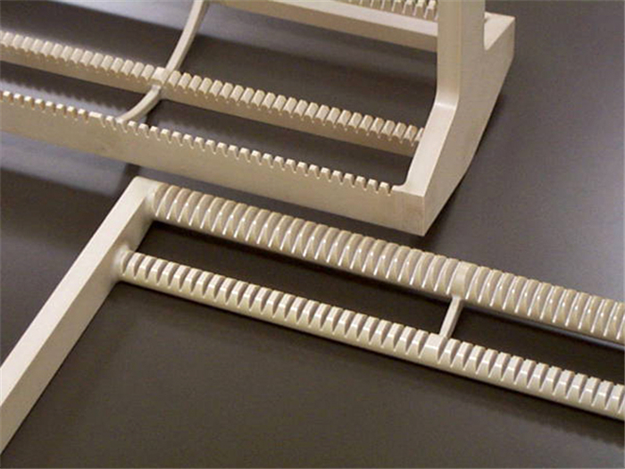
Wafer carriers are used to load wafers, including wafer carrier boxes, wafer transfer boxes and wafer boats. The time wafers are stored in shipping boxes accounts for a large portion of the entire production process, and the material, quality, and cleanliness of the wafer box itself may have a greater or lesser impact on wafer quality.
Wafer carriers generally use high temperature resistance, excellent mechanical properties, dimensional stability, durability, antistatic, low outgassing, low precipitation and recyclable materials. PEEK can be used to make carriers for general transport processes. Antistatic PEEK is generally used. PEEK has many excellent properties, such as abrasion resistance, chemical resistance, dimensional stability, antistatic and low outgassing, which help prevent particle contamination. And improve the reliability of chip processing, storage and transfer.
Materials include: PEEK, PFA, PP, PES, PC, PEI, COP, etc., generally after antistatic modification
3. Mask box
A photomask is a pattern master used in the photolithography process in chip manufacturing. It is based on quartz glass and coated with chrome metal to block light. Using the principle of exposure, the light source is projected onto the silicon wafer through a photomask to expose and display specific patterns. Any dust or scratches adhering to the photomask will degrade the quality of the projected image. Therefore, it is necessary to avoid contamination of the photomask and prevent particles generated by impact or friction from affecting the cleanliness of the photomask.
To avoid photomask damage due to fogging, friction or displacement, photomask pods are generally made of antistatic, low outgassing, durable materials.
PEEK has the characteristics of high hardness, very little particle generation, high cleanliness, antistatic, chemical corrosion resistance, wear resistance, hydrolysis resistance, good dielectric strength and good radiation resistance. And during reticle processing, reticle chips can be stored in an environment with low outgassing and low ionic contamination.
Material: anti-static PEEK, anti-static PC, etc.
4. Wafer tools
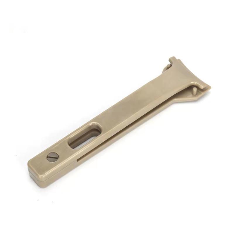
Tools for clamping wafers or silicon wafers, such as wafer clamps, vacuum suction pens, etc., when clamping wafers, the materials used will not scratch the wafer surface and have no residue, ensuring the integrity of the wafer surface cleanliness.
PEEK has the characteristics of high temperature resistance, wear resistance, good dimensional stability, low outgassing rate, and good hygroscopicity. When clamping wafers and wafers with PEEK wafer clamps, there will be no scratches on the wafer or wafer surface. Scratching does not cause residue on wafers and wafers due to friction, improving the surface cleanliness of wafers and wafers.
Material: PEEK
5. Semiconductor package test socket
A test socket is a device that electrically connects the direct circuit of each semiconductor component to a test instrument. Different test sockets are used to test various microchips specific to the IC designer. The material used for the test socket should meet the requirements of good dimensional stability, high mechanical strength, less burr formation, good durability, wide temperature range, and easy processing.
Material: PEEK, PPS, PAI, PI, PEI

For any inquiry please contact sales@honyplastic.com or WhatsApp (86)18680371609
November 17, 2024
November 16, 2024
August 27, 2021
August 26, 2021
PEEK ball is a special type of ball made of polyether ether ketone (PEEK), which has excellent chemical stability, abrasion resistance, and high temperature resistance.PEEK ball is widely used in...
PVDF Application Areas Different models of PVDF products are suitable for different application scenarios. According to application fields, PVDF can be divided into conventional grade products and...
Application Performance Advantages of MC nylon MC nylon is a new type of engineering plastics, due to its outstanding comprehensive performance, so that its status in engineering plastics is rapidly...
Types of nylon: 1. Nylon - 6 (PA6) Nylon -6, also known as polyamide -6, that is, polycaprolactam. Translucent or opaque opalescent resin. 2. Nylon - 66 (PA66) Nylon-66, also known as polyamide-66,...
Email to this supplier
November 17, 2024
November 16, 2024
August 27, 2021
August 26, 2021

Privacy statement: Your privacy is very important to Us. Our company promises not to disclose your personal information to any external company with out your explicit permission.

Fill in more information so that we can get in touch with you faster
Privacy statement: Your privacy is very important to Us. Our company promises not to disclose your personal information to any external company with out your explicit permission.